Trellisign Microelectronics Solutions
Comprehensive Microelectronics Solutions
Comprehensive Microelectronics Solutions
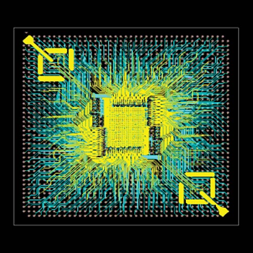
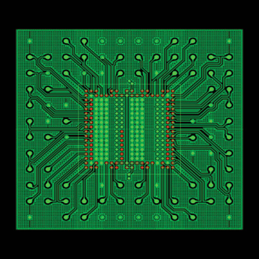
As VLSI designs grow in complexity with billions of transistors, advanced power constraints, and multi-million gate logic, traditional simulation methods struggle with:

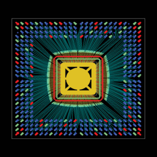
VLSI circuit simulation is a crucial step in semiconductor design that validates functionality, timing, and power behavior before fabrication. VLSI provides high-performance simulation solutions, such as Logic Simulator, which offer fast, scalable, and accurate verification for RTL-to-gate-level designs. These tools ensure early bug detection, reducing costly iterations and accelerating time-to-market.

Logic Simulator offers fast and efficient RTL and gate-level simulation.
Supports Verilog, System Verilog, VHDL, and mixed-language environments.
Advanced waveform analysis, assertions, and functional coverage support.
Works natively with EDA tools for complete design flow.
Advanced Simulation Features
Traditional circuit simulation focuses on verifying basic functionality but does not account for component variations, design optimization, or long-term reliability. Engineers face challenges in:

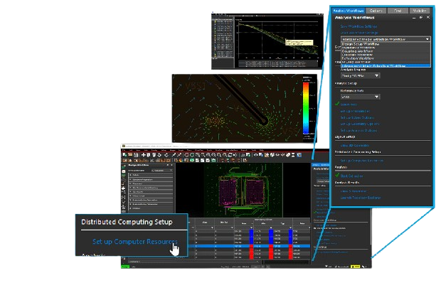
Advanced Analysis provides powerful simulation techniques for circuit optimization, sensitivity analysis, reliability testing, and parametric exploration. It helps engineers improve circuit robustness, optimize performance, and assess worst-case scenarios under real-world variations
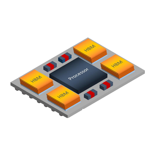
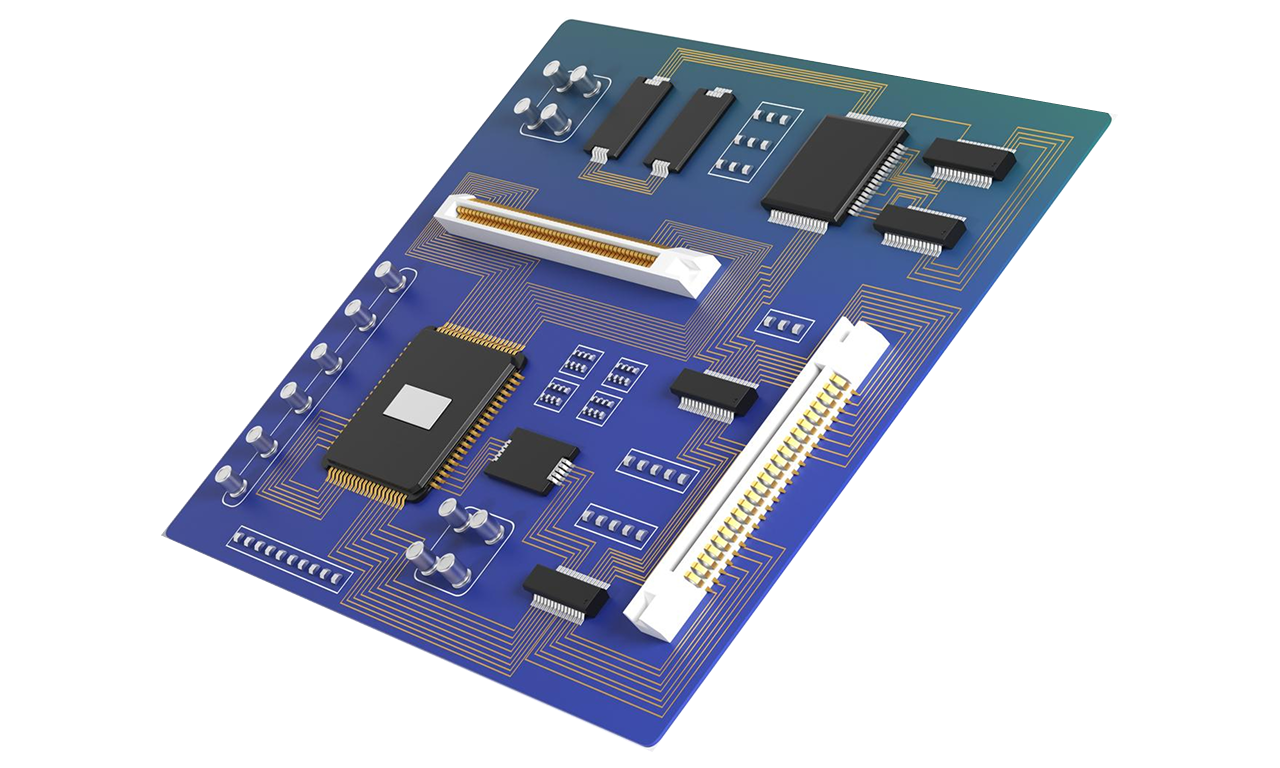
Traditional IC packaging methods face limitations in terms of performance, power consumption, and miniaturization. As semiconductor technology scales, there is a growing need for high-density integration, improved thermal management, and better electrical performance. Conventional packaging solutions struggle to meet these demands, necessitating the adoption of advanced packaging techniques.
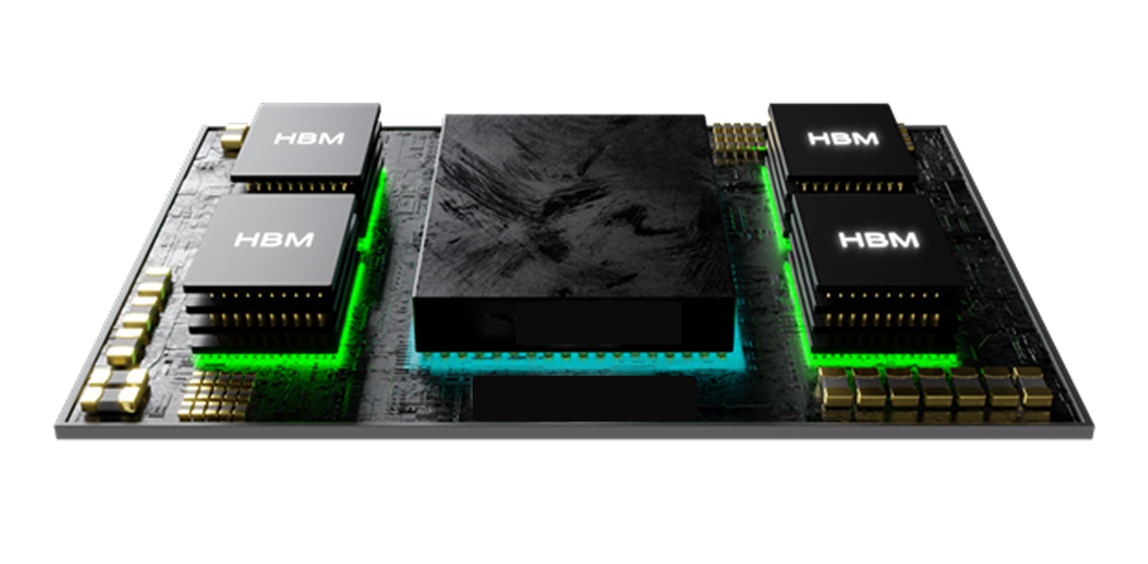
Traditional IC packaging methods face limitations in terms of performance, power consumption, and miniaturization. As semiconductor technology scales, there is a growing need for high-density integration, improved thermal management, and better electrical performance. Conventional packaging solutions struggle to meet these demands, necessitating the adoption of advanced packaging techniques.
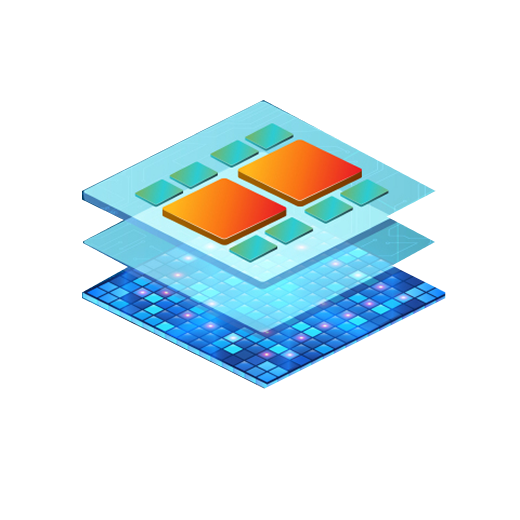
Seamless integration of IC, package, and PCB design.
Thermal, electrical, and mechanical simulations.
Ensures manufacturability and compliance.
Enables heterogeneous system designs.

Trellisign offers various bundles to enhance design capabilities in VLSI chip design, catering to different segments such as research, standard, and packaging. These bundles include comprehensive toolsets for Digital Physical Design, Simulation, and Timing Analysis, enabling users to leverage industry-leading design methodologies and IP.
Our portfolio offers resources over the entire spectrum of VLSI Chip Design Life Cycle to the academia, covering the following:
Cadence University Bundle: Empowering academia and research institutions, Cadence University Bundle provides cutting-edge tools for exploring advanced semiconductor designs and systems. Tailored for innovative projects, this bundle supports state-of-the-art simulation, verification, and layout solutions to foster breakthroughs in electronic design automation.
Packaging Bundle: The Packaging Bundle enables streamlined chip-package-board co-design with integrated tools for IC packaging, thermal analysis, and signal/power integrity. It addresses the growing complexity of modern electronics, ensuring optimized designs and faster time to market.
Application Engineers at Trellisign play a critical role in helping customers successfully implement and optimize Cadence’s EDA tools and solutions. They provide technical expertise, support, and training to ensure seamless integration into design workflows. They bridge the gap between customer needs and product development.
Collaborating closely with customers to identify and address their design challenges.
Creating custom solutions and designs using Cadence’s cutting-edge software tools.
Providing ongoing support and resolving any issues that arise after the sale of tools.
Gathering customer feedback to provide valuable insights for product improvement.
Installation Support for EDA Tools ensures seamless deployment of electronic design automation (EDA) software by assisting users with the setup, configuration, and troubleshooting of the tools.
Verifying that customer hardware and operating systems meet tool requirements.
Assisting in configuring FlexNet license servers and managing license files.
Guiding users through the step-by-step installation process for EDA tool products.
Configuring shell environments (.bashrc, .cshrc) for proper tool execution.
Troubleshooting issues such as missing dependencies, path errors, or license-related problems.
Supporting the installation of patches and new tool releases to ensure performance and feature enhancements.
Providing manuals, FAQs, and training for self-installation and configuration.
UTB is a curated series of lab-based experiments sourced from leading universities across India. Designed to bridge the gap between theoretical knowledge and real-world applications, UTB enhances learning through hands-on training, visual demonstrations, and expert-led sessions.
Whether you're a student, educator, or industry professional, UTB equips you with practical skills and domain expertise essential for tackling real-world challenges.
UTB sessions provide practical experience with industry-standard tools which enables students to apply theoretical concepts in real-world scenarios.
Guidance from mentors helps students navigate complex design & analysis tasks, fostering a deeper understanding of the subject matter.
The program covers a wide range of topics, from ASIC design and verification to diverse engineering disciplines.
Recorded sessions and supplementary materials are available for students to review and reinforce their learning at their own pace.
