Flip Chip Technology: The Backbone of Modern High-Performance Semiconductor Packaging
As semiconductor devices continue to become smaller, faster, and more powerful, packaging technology has evolved significantly to meet increasing electrical, thermal, and mechanical demands. One of the most important breakthroughs in advanced semiconductor packaging is Flip Chip Technology
From smartphones and gaming GPUs to artificial intelligence accelerators and automotive electronics, flip chip packaging has become a preferred solution for achieving high-speed performance, compact size, and efficient heat dissipation.
What is Flip Chip Technology?
Flip chip is an advanced semiconductor packaging method in which the silicon die is mounted upside down directly onto the substrate or PCB using tiny solder bumps instead of traditional bonding wires.
In conventional packaging, electrical connections are made using thin gold or copper wires attached around the edges of the chip. In flip chip packaging, the die is literally “flipped,” allowing the solder bumps distributed across the entire chip surface to connect directly with the substrate.
This structure provides:
- Shorter electrical paths
- Higher I/O density
- Lower signal delay
- Better thermal conductivity
- Smaller package size
Evolution of Flip Chip Technology
The evolution of semiconductor packaging has progressed through several important stages:
Through-Hole and DIP Packaging Era
Early semiconductor devices used large packages with long interconnections. Performance requirements were relatively low.
Surface Mount Technology (SMT)The industry moved toward smaller and lighter packages such as QFP and BGA to improve PCB density.
Wire Bonding DominanceWire bonding became the standard interconnection technology for decades because of its simplicity and lower manufacturing cost.
Introduction of Flip Chip (C4 Technology)IBM introduced Controlled Collapse Chip Connection (C4), which became the foundation of modern flip chip packaging.
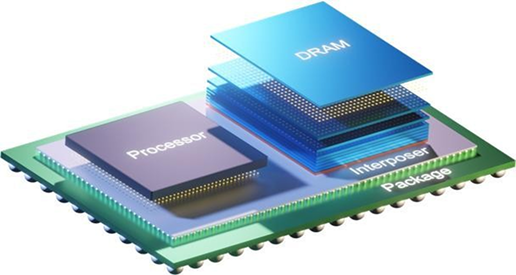
Advanced Packaging EraModern packaging now includes:
- Flip Chip BGA (FC-BGA)
- 2.5D Packaging
- 3D IC Integration
- Chiplet Architectures
- Wafer Level Packaging (WLP)
These technologies are heavily used in AI processors, HPC systems, and 5G devices.
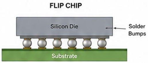
A typical flip chip package contains:
- Silicon Die – the actual semiconductor chip
- Solder Bumps – tiny conductive bumps formed on chip pads
- Substrate – routes electrical signals to the PCB
- Underfill Material – epoxy material added for mechanical reliability
- BGA Balls – second-level interconnect to PCB
Wire Bonding vs Flip Chip Technology
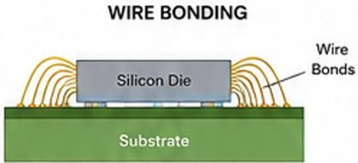
What is Wire Bonding?
Wire bonding is a traditional packaging method where thin gold, copper, or aluminum wires connect the die pads to the package leads.
Although it remains widely used for low-cost applications, its limitations become significant in high-speed and high-power designs.
Comparison Between Wire Bonding and Flip Chip
| Feature | Wire Bonding | Flip Chip |
| Connection Method | Thin bonding wires | Solder bumps |
| Interconnect Type | Peripheral connection | Area-array connection |
| Electrical Performance | Moderate | Excellent |
| Signal Delay | Higher | Lower |
| Thermal Performance | Moderate | Superior |
| I/O Density | Limited | Very High |
| Package Size | Larger | Compact |
| Manufacturing Cost | Lower | Higher |
Why Flip Chip is Better for High-Performance Devices
- Shorter Electrical Path
The shorter bump connections reduce parasitic inductance and resistance, enabling faster signal transmission - Better Thermal Dissipation
Heat can flow directly from the backside of the die to the heat sink, making flip chip ideal for high-power processors. - Higher I/O Density
Because bumps are distributed across the entire die surface, thousands of connections can be achieved within a compact area. - Smaller Form Factor
Flip chip eliminates the need for long bonding wires and large peripheral pad rings.
Manufacturing Process of Flip Chip Packaging
Wafer Bumping
Tiny solder bumps are deposited on the die pads.
Die Flip and Alignment
The die is flipped upside down and aligned precisely with the substrate.
Reflow Process
Heat melts the solder bumps to form electrical and mechanical connections.
Underfill Application
Epoxy underfill is injected between die and substrate to improve reliability.
Final Assembly and Testing
The package undergoes electrical and thermal testing.
Real-World Applications of Flip Chip Technology
Flip chip packaging enables compact, high-performance, and reliable semiconductor solutions across multiple industries.
Consumer Electronics
- Smartphones
- Tablets
- Smartwatches
- Gaming Consoles
Modern mobile processors require compact packaging, low power consumption, and high-speed signal performance.
Artificial Intelligence & Data Centers
- Faster Communication
- Better Cooling
- Higher Reliability
AI accelerators generate significant heat and require extremely high bandwidth for modern computing workloads.
Automotive Electronics
- ADAS Systems
- Radar Modules
- Autonomous Driving Processors
- EV Control Systems
Reliable semiconductor packaging for safety-critical automotive applications and harsh environments.
Networking & 5G
- High-Frequency RF Systems
- Signal Integrity
- Low Latency Communication
Supports advanced RF and high-frequency networking applications where performance is critical.
Cost Analysis of Flip Chip Technology
While flip chip packaging requires a higher initial investment, its performance and scalability often result in long-term cost advantages.
Why Flip Chip is Expensive
- Wafer Bumping Process
- High-Precision Alignment Tools
- Advanced Substrates
- Underfill Materials
- Complex Inspection Methods
Flip chip packaging generally costs more
When Flip Chip Becomes Cost Effective
Although initial manufacturing cost is higher, flip chip becomes economical for:
- High-Volume Production
- High I/O Devices
- Advanced Processors
- High-Performance Applications
This is because smaller die size and improved performance can offset packaging costs.
Challenges in Flip Chip Technology
Despite its advantages, flip chip packaging introduces several technical and manufacturing challenges.
Thermal Expansion Mismatch
Different materials expand at different rates under temperature variation, leading to mechanical stress and reliability concerns.
Complex Manufacturing
Requires precise alignment, bump formation, and advanced equipment to ensure micron-level accuracy.
Difficult Rework
Once underfill is applied, repairing or reworking the package becomes extremely difficult and costly.
Inspection Complexity
Electrical connections are hidden under the die, requiring advanced X-ray and imaging techniques for inspection.
Future of Flip Chip Technology
The future of semiconductor packaging is strongly driven by advanced integration, miniaturization, and AI-powered computing.
Chiplet Architecture
Instead of a single large die, multiple smaller dies are interconnected within one package for better yield and flexibility.
2.5D & 3D Packaging
Vertical stacking improves bandwidth, reduces latency, and enhances overall system performance.
Copper Pillar Interconnects
Replacing solder bumps with copper pillars enables finer pitch, improved current handling, and better reliability.
Heterogeneous Integration
Combines logic, memory, and RF devices into a single package for highly optimized system design.
AI & HPC Growth
The rise of AI and high-performance computing continues to accelerate demand for advanced flip chip packaging solutions.
Conclusion
Flip chip technology has transformed the semiconductor packaging industry by enabling compact, high-speed, and thermally efficient electronic systems. While traditional wire bonding remains relevant for low-cost and low-performance devices, flip chip packaging has become essential for modern applications such as CPUs, GPUs, AI accelerators, 5G infrastructure, and automotive electronics
To continue reading the entire blog