Trellisign Electronic Design Automation (EDA)


Trellisign Electronic Design Automation (EDA)

The global electronics sector continuously evolves toward more compact, high-performance, and dependable systems. Engineering professionals today confront multifaceted obstacles spanning chip architecture, printed circuit board implementation, sophisticated packaging methodologies, and holistic system integration—while operating under relentless time-to-market constraints.

Our integrated electronic design automation platform delivers end-to-end solutions from discrete semiconductor elements to complete system frameworks. These battle-tested technologies are distinguished by their exceptional scalability, engineering precision, and proven track record of first-silicon success across diverse applications.


Chip Design & Verification Technologies (VLSI)

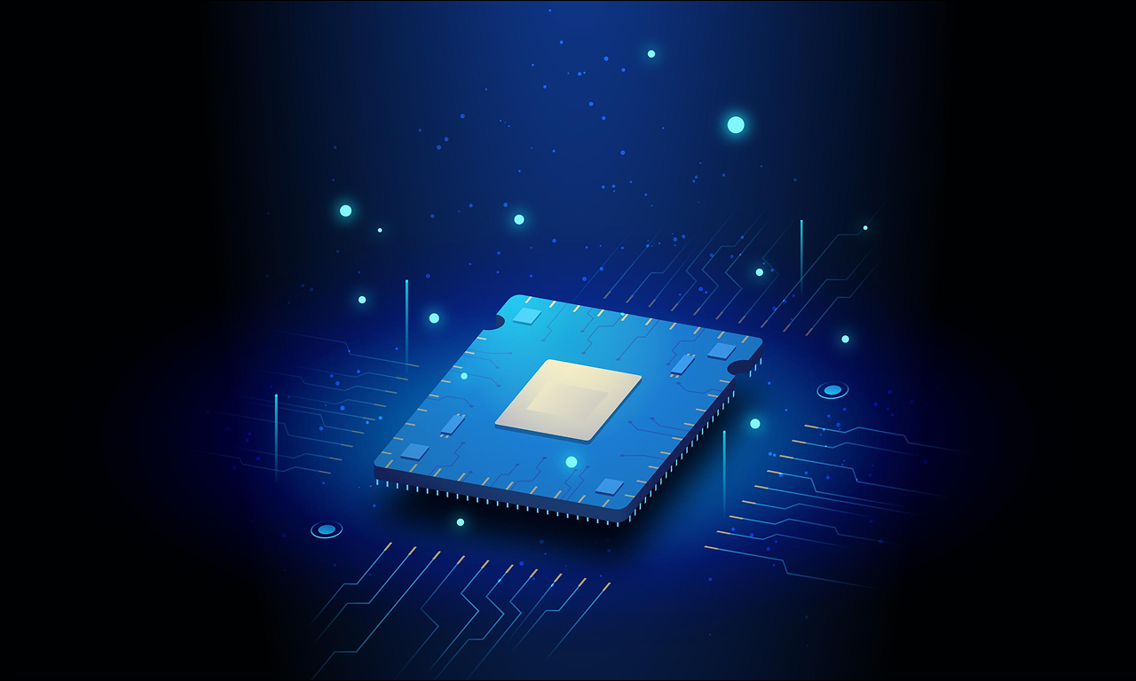
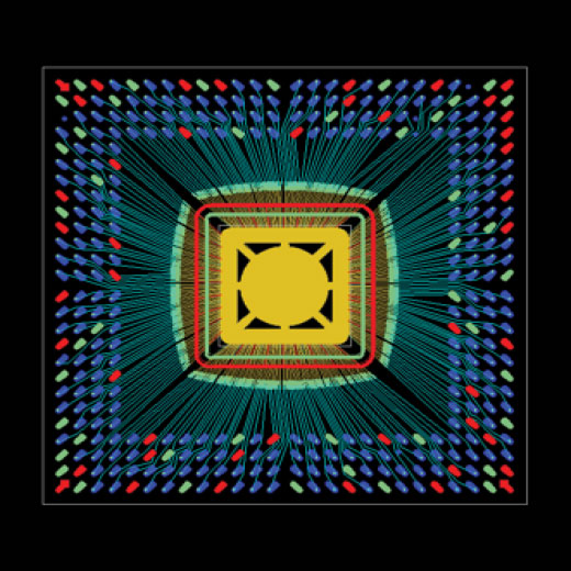
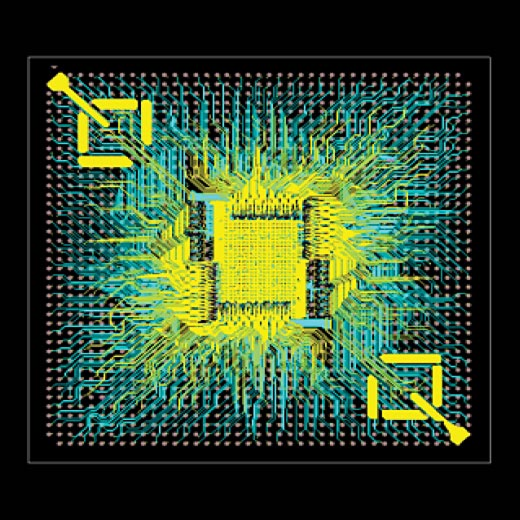
Today's semiconductor architectures integrate tens of billions of transistors using state-of-the-art fabrication processes and complex heterogeneous designs. Achieving optimal power consumption, performance targets, and die area utilization while ensuring manufacturability creates significant engineering complexity. Conventional design approaches frequently struggle to meet the demands of such extensive integration requirements.

VLSI Platform Challenges

Our Methodology

Our chip design framework delivers end-to-end workflows that ensure design efficiency, accuracy, and fabrication success.

  • Complete RTL-to-GDSII Workflows
    • Covering digital, analog, and mixed-signal circuits — from register-transfer-level design to mask-ready layouts
  • AI-Enhanced Optimization
    • Advanced artificial intelligence engines accelerate convergence and optimize power, performance, and area (PPA)
  • Fab-Certified Validation
    • Verification flows aligned with leading foundries to ensure compliance and manufacturability at advanced nodes
  • Accelerated Design Closure
    • Integrated signoff methodologies reduce cycle time while improving design quality and reliability
  • Hybrid Design Capability
    • Seamless support for digital, analog, and hybrid circuit implementations within a unified environment
  • First-Pass Silicon Success
    • Combining automation, proven algorithms, and certified methodologies to minimize re-spins and enhance fabrication success rates

Key Features

Rapid Development

Machine learning-driven workflows minimize design iterations

Optimal Performance

Advanced power, speed, and area optimization for leading-edge nodes

Reduced Risk

Thorough verification minimizes expensive silicon revisions

Logic Simulator Technical Specifications

Technology Highlights

  • Complete design environment accommodating all circuit architectures
  • Advanced timing, power analysis, and reliability assessment with integrated signal/power integrity validation
  • Native support for chiplet-based and three-dimensional semiconductor assemblies
  • Market-leading capabilities for emerging fabrication technologies

Printed Circuit Board Engineering & Analysis Platform (PCB)

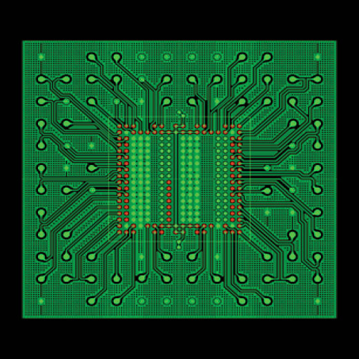
Contemporary PCB implementations face escalating design constraints: increased component integration density, high-speed signal routing requirements, and stringent compliance mandates. Engineering errors during schematic creation, physical routing, or manufacturing validation phases can result in substantial project delays and product quality issues.

  • Identifying critical components affecting performance
  • Finding optimal component values for efficiency
  • Analysing circuit behavior under real-world variations
  • Ensuring reliability and avoiding component failures
VLSI Platform Challenges

Our Methodology

Our PCB engineering solution provides a rule-based, scalable workflow that supports everything from simple prototypes to enterprise-grade high-speed systems.

  • Circuit Capture & Schematic Entry
    • Robust schematic design tools with constraint-driven capture for error-free logic definition.
  • Physical Implementation
    • Automated and manual layout capabilities with design rule enforcement to meet electrical and manufacturing constraints.
  • Comprehensive Verification
    • Built-in DRC, ERC, and SI/PI analysis to validate functionality, manufacturability, and reliability before fabrication.
  • Rule-Based Expandable Architecture
    • Scalable platform that adapts to projects of varying complexity — from entry-level designs to advanced multi-layer boards.
  • Prototype-to-Production Ready
    • Seamless transition from early-stage prototypes to full-scale enterprise designs without workflow disruption.

Key Features

Accelerated Time-to-Market

Optimized design flow and rapid production qualification

Superior Precision

Continuous manufacturing validation with automated design rule verification

Universal Adaptability

Single platform architecture supporting entry-level through enterprise applications

Logic Simulator Technical Specifications

Technology Highlights

  • Advanced schematic entry with intelligent physical layout automation
  • Dynamic three-dimensional modeling with real-time manufacturability assessment
  • Comprehensive high-speed design capabilities featuring integrated signal integrity and power integrity optimization with impedance management
  • Complete solution ecosystem from economical starter tools to premium enterprise systems

Sophisticated IC Packaging Technologies (IC PACKAGING)

With conventional transistor scaling reaching fundamental physical barriers, performance enhancements increasingly rely on advanced packaging innovations including 2.5D/3D stacking and multi-technology integration approaches. Design complications discovered during late packaging phases can generate significant cost overruns and schedule impacts.

VLSI Platform Challenges

Our Methodology

  • Comprehensive Substrate Engineering
    • Advanced substrate design capabilities for complex multi-layer packaging architectures
  • Unified Co-Optimization
    • Integrated chip-package-system design methodology ensuring optimal performance across all domains
  • Multi-Physics Analysis
    • Simultaneous thermal, electrical, and mechanical validation for comprehensive design verification.

Key Features of Integrated Design Environment

Faster Product Launch

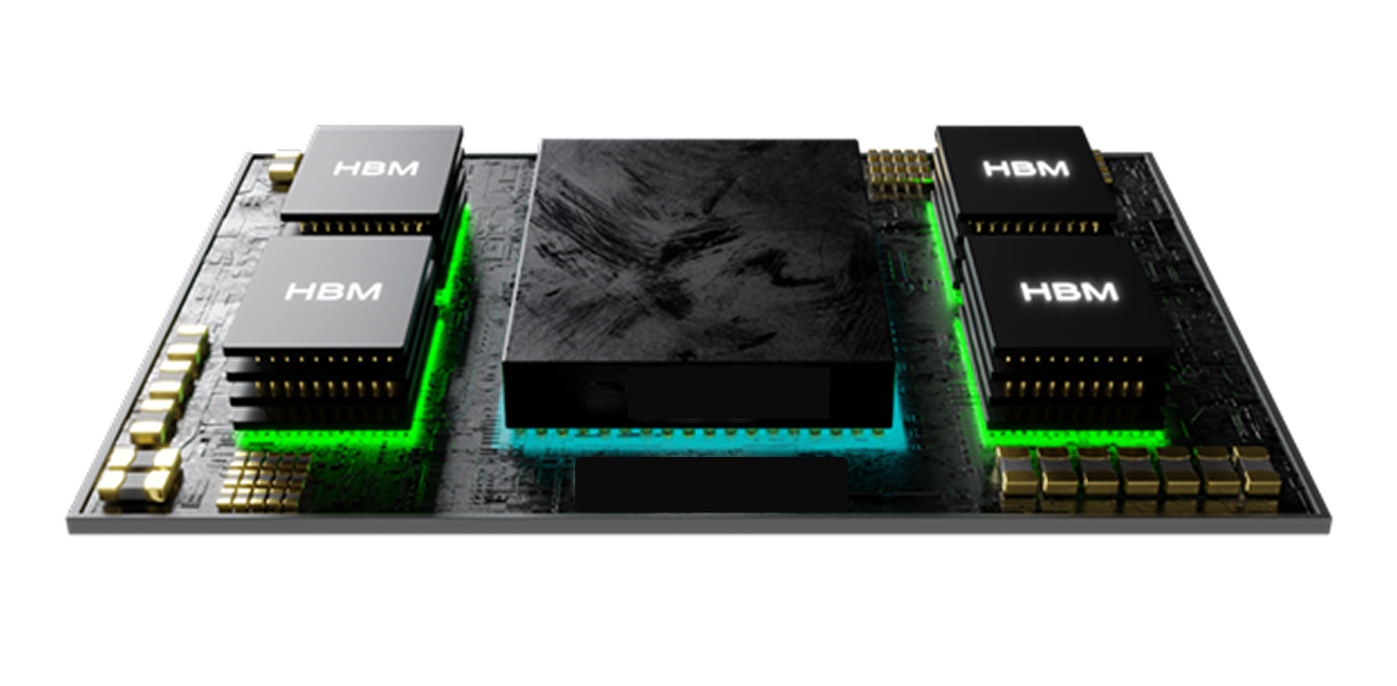
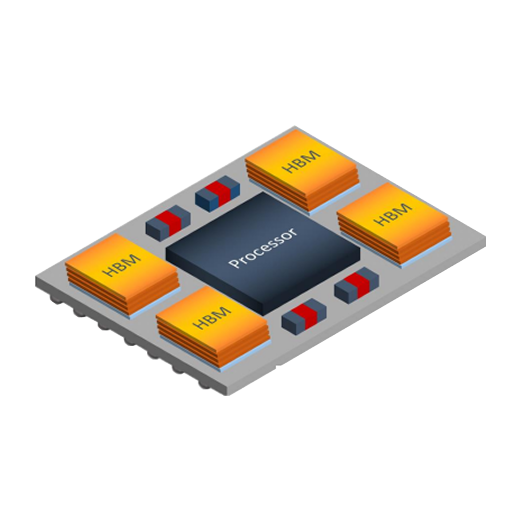
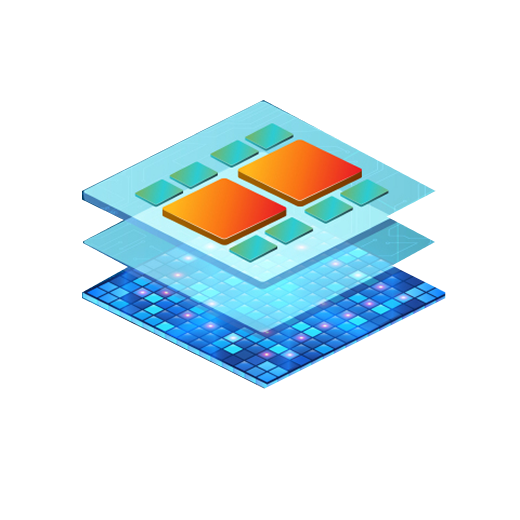
Unified co-engineering methodology accelerates development timelines

Comprehensive Performance Optimization

Superior characteristics across thermal, electrical, and mechanical parameters with embedded SI/PI verification

Design Optimization

Advanced packaging design validation ensures optimal performance characteristics.


Technical Specifications

Technology Highlights

  • Full-featured packaging design environment
  • Integrated signal integrity and power integrity optimization for package-level performance enhancement
  • Multi-physics thermal, electrical, and mechanical validation capabilities
  • Seamless chip-package-board co-design workflow integration

Contact us

For below details

  • Technical Specification Details
  • Platform Architecture
  • Integration Guide
  • Case Study Insights
  • or more


Email us at

info@trellisign.com

Success

Thank you for your submission!

We will get back to you soon

Server error: Please try again after some time.